Scanning Electron Microscopy (SEM)
In the dance of electrons, we uncover the hidden stories etched upon the tiniest canvases, expanding our understanding of the universe, one magnified detail at a time.
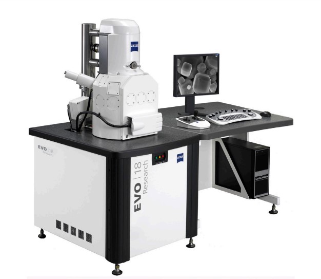
The scanning Electron Microscopy Lab of the Nuclear Science and Engineering Department (MIST), Bangladesh is equipped with a cutting-edge ZEISS EVO 18 model.
Within these walls is a realm where the hidden is revealed and the most minute details are revealed with astounding clarity and accuracy. Our cutting-edge facility is committed to pushing the limits of technical innovation and scientific discovery as we investigate the mysteries of the microscopic world.
Our team of committed researchers, academics, and technicians works relentlessly to solve the riddles shrouded at the microscale while immersed in the soothing hum of scientific investigation. Our SEM lab serves a wide range of scientific fields and commercial applications, from examining the complex structures of both conductive and non-conductive specimens to examining the surface characteristics, and material characterization of industrial materials.
Our SEM lab serves as a hub for collaboration and knowledge sharing in addition to being a place for scientific research. We warmly invite academics, students, and members of the business community to explore the limitless possibilities of scanning electron microscopy, participate in multidisciplinary discussions, and set out on enlightening research journeys.
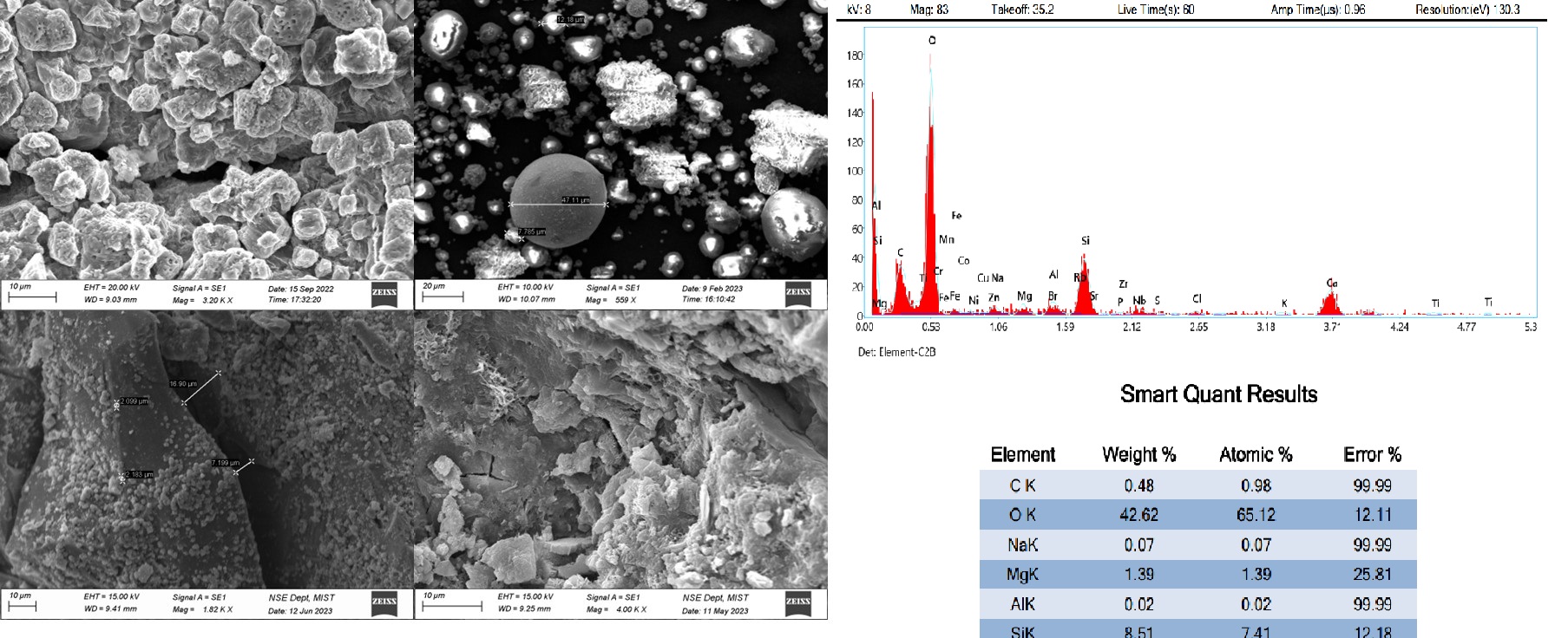
SEM Sample Result (Morphology and Elemental Analysis)
Specification
| Resolution | 3 nm at 30 KV SE |
| Acceleration Voltage | 0.2 to 30 KV |
| Probe Current | 0.5 pA to 5 µA |
| Magnification | < 5 - 1,000,000x |
Our Services
- Gold coating of biological samples
- Imaging of industrial materials
- Imaging of biological samples
- Elemental Analysis
Test Rates
|
Test Name |
Rate (BDT) (For MIST Students and Faculty) |
Rate (BDT) (Others) |
|
Imaging of conductive material |
1200 |
3000 |
|
Imaging of non-conductive material |
1300 |
3000 |
|
Elemental Analysis using EDX |
2000 |
4000 |
|
Elemental Analysis using EDX (With Mapping) |
3500 |
5500 |
Query (For Appointment)
- Lab In-Charge-1: Fahim Sabab Siddique (Lecturer)
Contact: +8801921998429
Email: fahim@nse.mist.ac.bd
- Lab In-Charge-2: Razia Sultana Ripa (Lecturer)
Contact: +880168193929
Email: razia@nse.mist.ac.bd
- Program Coordinator: Major Selina Nasrin, Engrs
Contact: +8801769024176
Email: prog.coordinator@nse.mist.ac.bd